Swinging for the fences
The term “particle accelerator” might lead most people to envision long underground tunnels stretching tens of kilometers and rooms full of large, bulky devices, but for years, researchers around the world have been pursuing smaller, lower cost and more efficient alternatives that have myriad potential applications in various scientific and medical fields. The Moore Foundation has funded such an effort for the past eight years through the Accelerator on a Chip, or ACHIP, international project to create a dielectric laser accelerator. In 2023, teams of physicists at Friedrich-Alexander-Universität Erlangen-Nürnberg (FAU) and Stanford University published papers demonstrating nanophotonic electron accelerators.
Ten years earlier, Robert Byer at Stanford was struggling to find adequate support for his dielectric laser accelerator research after losing DARPA funding. At the same time as losing funding, Byer’s group at Stanford and Peter Hommelhoff’s at FAU both independently published papers demonstrating successful particle acceleration at an individual nanostructure. While their work was ambitious and promising, the difficulty and risk involved were clear obstacles to finding the right financial backing. In 2015, Moore Foundation science Program Officer Gary Greenburg worked with Byer and Hommelhoff to put together an international team of universities, national laboratories and industrial partners to continue funding the work. This new group now had the funding to start tackling the big open issues of how to truly build an accelerator on a chip.

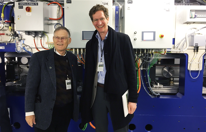
[Image] Moore Foundation's Accelerator on a Chip co-principal Investigators Bob Byer (left) and Peter Hommelhoff (right).
At the time of funding, the idea of a miniature particle accelerator seemed far-fetched to many in the research community. However, the groundwork established by those previously published studies left Greenburg confident that the science was sound, and that the expertise of the team and incredible potential impact of the project justified “swinging for the fences,” as Gordon Moore once said. “These multi-institutional types of projects with difficult science and complex engineering can take many years to be successful,” Greenburg said, “but perseverance, dedication and skilled project management by the grant team reduces the scientific risk.”
Ultimately, the ACHIP team was given the time and runway necessary to produce results.
The key difference in the design of ACHIP from conventional particle accelerators is that ACHIP uses the electric field of a laser instead of microwaves to accelerate electrons. These fields can be much stronger, and, when properly synchronized, can lead to astonishing gains in particle energy. For ACHIP, the electrons travel down a tiny 400nm channel formed by a series of nano-pillar structures (Figure 1 b, c) in a silicon chip (Figure 1a) while in a conventional accelerator the electrons travel through a four-inch copper tube that is surrounded by large magnets. This compact arrangement may result in wholly new applications of accelerators but requires very precise steering of the electron beam.

[Image] Figure 1: The silicon accelerator on a chip (a) measures 1 mm in length; (b) Electron micrograph of the accelerator chip pillar structure; (c) electron beam travels down a 400nm channel between the pillars through which the electrons are accelerated by a laser beam.
Over the past several years, the project connected researchers from institutions across the world – in addition to the groups from the United States and Germany, Israeli and Japanese labs also played a large role. These groups all brought slightly different, complementary expertise that helped move ACHIP along over regular, well-organized international meetings and collaboration guided by an advisory committee. Mitsuru Uesaka’s lab at Tokyo University brought unique expertise in understanding how electrons interact with atoms or solids under the presence of laser fields and designing new experiments. While Ido Kaminer’s group at the Technion in Israel contributed their expertise on conducting ultrafast transmission electron microscope experiments. “This is something that’s so beautiful about science,” Hommelhoff said. “It can relatively easily unite the world, because the laws of physics are the same wherever you are. These days, that carries a lot of value.”
In the long term, Hommelhoff hopes to see the research result in a product that can be used in a variety of areas including medical treatment and diagnosis – miniature particle accelerators could open up new cancer treatment tools, such as treating skin cancer with an electron beam. Or new ways to take X-rays inside a patient’s body could create new diagnostic tools.
The project has also opened up several new research pathways including one to image quantum coherence using an accelerator on a chip as a way to shape the electron beam. This new imaging approach produces electrons with a modulated wave function allowing for the extraction of entirely new information from a sample.
Of course, this just scratches the surface of potential applications. It is hard to anticipate all the potential uses of this technology over the long term, but the field is primed for growth and innovation over the next several years. “Slowly, the accelerator world is understanding the importance of ACHIP,” Byer said. “The quantum world has already made significant progress in the study of electrons entangled with the dielectric accelerator structure. I am patiently waiting for the first ACHIP Free Electron Laser on a chip. It will happen.”

Message sent
Thank you for sharing.